TVS Transistor (Surge Protector) Core Parameters and Selection Guide
TVS transistors (transient voltage suppressors) are core components for suppressing circuit surges and protecting electronic devices. The key to selection is matching the voltage, current, and power parameters of the application scenario, while also considering response characteristics and circuit compatibility. Incorrect parameter selection can lead to protection failure or false triggering. Below are the key parameters and system selection methods that require attention.
I. Key TVS Transistor Parameters to Focus On
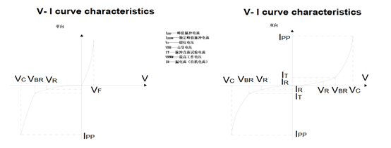
When a TVS transistor is subjected to a reverse transient high-energy surge, it can change the high impedance between its terminals to a low impedance within a maximum speed of 1 ns, clamping the voltage between its terminals to a predetermined value, effectively protecting the precision components in the electronic circuit. Under surge voltage, the voltage across the TVS diode rises from the rated reverse turn-off voltage VRWM to the breakdown voltage VBR, causing it to break down. With the appearance of the breakdown current, the current flowing through the TVS diode reaches its peak pulse current IPP, and the voltage across it is clamped below the predetermined maximum clamping voltage VC. Subsequently, as the pulse current decays exponentially, the voltage across the TVS diode also decreases continuously, eventually returning to its initial voltage. TVS diodes are available in unidirectional and bidirectional types. The characteristics of a unidirectional TVS diode are similar to those of a Zener diode, while the characteristics of a bidirectional TVS diode are equivalent to two Zener diodes connected in reverse series. The following diagram illustrates their relationship.
1. Reverse Cut-off Voltage (VRWM) �C Core Matching Parameter
Definition: The maximum reverse DC/AC voltage (RMS value for AC) that a TVS diode can continuously withstand when it is in the off state; also called the maximum operating voltage.
Crucial Function: It must be greater than the rated operating voltage of the protected circuit; otherwise, the TVS diode will remain in a slightly conductive state for a long time, overheating or even burning out. It also cannot be too high, otherwise, the protection sensitivity will be reduced.
Selection Notes:
DC Circuit: VRWM �� 1.1~1.2 times the rated operating voltage of the circuit (allowing for derating margin);
AC Circuit: VRWM �� 1.414 times the RMS value of the AC rated voltage (covering peak value).
2. Breakdown Voltage (VBR) �C Turn-on Threshold
Definition: The minimum reverse voltage at which the TVS diode begins to break down and conduct, discharging surge current (test current is usually 1mA), with tolerances of ��5%/��10%.
Key Function: VBR should be slightly higher than VRWM and lower than the maximum withstand voltage of the protected device (such as the ESD withstand voltage of an IC or the withstand voltage of a capacitor) to ensure that it breaks down before the protected device when a surge occurs.
Selection Note: The actual value of VBR must fall between the "upper limit of the circuit operating voltage" and the "lower limit of the withstand voltage of the protected device".
3. Clamping Voltage (VC) �C Core Protection Indicator
Definition: The maximum voltage across the TVS diode under peak pulse current (IPP) (i.e., the voltage that the protected circuit actually withstands when a surge occurs).
Key Function: It must be �� the maximum transient voltage that the protected device can withstand (such as V(ESD) and V(surge) in the device datasheet), otherwise the device will still be damaged by the surge.
Selection Note: VC is positively correlated with IPP; the VC value under the corresponding surge current must be confirmed, not the no-load value.
4. Peak Pulse Current (IPP) �C Surge Resistance
Definition: The maximum single pulse current a TVS diode can withstand (the pulse waveform is typically 8/20��s, the standard waveform for surge testing).
Key Function: Must be greater than the maximum surge current that may occur in the application scenario (e.g., power grid surges, electrostatic discharge, lightning-induced current).
Selection Note: For multiple surge impacts, the derating needs to be adjusted according to the pulse repetition frequency (e.g., for high-frequency surges, a model with a higher IPP is required).
5. Peak Pulse Power (PPP) �C Power Tolerance
Definition: Ppp = VC �� IPP (under 8/20��s waveform), representing the maximum power a TVS diode can withstand in a single surge.
Key Function: Must match the surge energy; insufficient power will cause the TVS diode to burn out instantly.
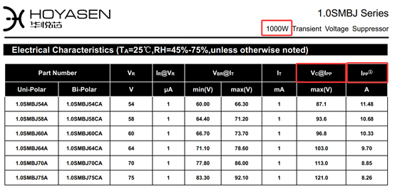
Selection Note: Larger packages generally have higher Ppp (e.g., Huayuexin 1.0SMB package approximately 1000W, DO-214AB approximately 1000W, high-power modules can reach several kilowatts).
6. Response Time �C Key to High-Speed Protection
Definition: The time it takes for a TVS diode to conduct and discharge current from the onset of a surge, typically in the picosecond (ps) range.
Key Function: Far superior to varistors (ns), suitable for high-frequency/high-speed circuits (such as communication interfaces, USB, HDMI). The response time must be less than the surge rise time.
Selection Note: For high-speed signal circuits (such as 5G, RF), TVS diodes with a response time �� 1ns are preferred.
7. Junction Capacitance (CJ) �C Core Limitation of High-Frequency Circuits
Definition: The junction capacitance of a TVS diode when reverse biased.
Key Function: Excessive junction capacitance can attenuate and distort high-frequency signals (such as RF, high-speed digital signals), and may even affect the normal operation of the circuit.
Selection Notes:
Low-frequency circuits (e.g., power supplies, mains signals): CJ is not strictly limited (tens of nF are acceptable);
High-frequency/high-speed circuits (e.g., RF, USB 3.0, Ethernet): Low junction capacitance TVS (CJ �� 1pF, even below 0.2pF) is required.
8. Polarity �C Compatible Circuit Type
Single-directional TVS: Effective only against reverse surges, suitable for DC circuits (e.g., power supply polarity protection);
Bidirectional TVS: Effective against both positive and negative surges, suitable for AC circuits (e.g., mains power) or non-polarity signal circuits (e.g., communication buses).
9. Packaging Forms �C Heat Dissipation and Mounting Fit
Surface Mount Packages: SMC, SMB, SMA, SMF, DFN, etc., suitable for miniaturized devices (consumer electronics, industrial control boards, BMS lithium battery protection boards). Heat dissipation capacity increases with package size.
Through-in Packages: P-600, DO-41, DO-15, DO-201, etc., suitable for high-power surge scenarios (industrial power supplies, power grid equipment), offering better heat dissipation.
Array Packages: TVS Array (e.g., ESD arrays), integrating multiple TVS diodes, suitable for multi-line protection (e.g., USB, HDMI interfaces), saving space.
II. TVS Transistor Selection Guide
Step 1: Define the Basic Operating Conditions of the Protected Circuit
Confirm Circuit Type: DC/AC, Low Frequency/High Frequency, Single-Channel/Multi-Channel;
Record Key Parameters: Rated Operating Voltage (Vwork), Maximum Operating Current, Maximum Transient Withstand Voltage of the Protected Device (Vmax);
Define Surge Environment: Surge Type (ESD, Lightning, Power Grid Fluctuation), Surge Peak Current (I_surge), Surge Waveform (e.g., 8/20��s, 10/1000��s).
Step 2: Match Reverse Cut-off Voltage (VRWM)
DC Circuit: VRWM �� 1.1 �� Vwork (Derating 10%~20% to prevent voltage fluctuations from causing TVS conduction);
AC Circuit: VRWM �� 1.414 �� Vwork (RMS value), for example, for a 220VAC circuit, VRWM �� 311V, but a 330V rating should be selected.
Step 3: Control Clamp Voltage (VC)
Ensure VC �� 0.8 �� Vmax (the withstand voltage of the protected device, then derating by 20%). For example, if the ESD withstand voltage of the MCU is 20V, then VC needs to be �� 16V.
Step 4: Calculate Peak Pulse Current/Power
IPP �� 1.2 �� I_surge (surge current drated by 20%), and verify that PPM = VC �� IPP �� surge power.
For recurring surges (such as frequent power grid fluctuations), additional derating is required: the actual IPP value should be �� 50% of the nominal value.
Step 5: Adapt Junction Capacitance and Frequency
High-frequency/high-speed circuits (such as 2.4G RF, USB 3.1): Select ultra-low junction capacitance TVS (such as SMF package, ESD array) with CJ �� 1pF.
Low-frequency circuits (such as 12V DC power supply): CJ can be ignored; prioritize power and voltage.
Step 6: Select Polarity and Package
DC unipolar circuits (e.g., 12V power supply positive terminal): Select unidirectional TVS;
AC/non-polar signals (e.g., Ethernet, AC mains): Select bidirectional TVS;
Miniaturized devices: Surface mount package (SMA/SMB); High-power scenarios: Through-hole package (DO-201) or TVS module.
Step 7: Verify Derating and Compatibility
Derating principle: Actual operating values of all parameters (voltage, current, power) �� 80% of nominal values;
Compatibility test: After selection, verify that the circuit works normally (e.g., whether the attenuation of high-frequency signals is within the allowable range), and that the TVS is undamaged and the protected devices function normally after surge testing.
III. Common Selection Misconceptions
Focusing solely on VRWM, ignoring VC: VC is the actual voltage the protected device withstands. Even with a matching VRWM, an excessively high VC can still damage the device.
Mismatched junction capacitance to frequency: Using a TVS with high junction capacitance in high-frequency circuits leads to signal distortion and packet loss.
No derating margin: Selecting directly based on rated values will cause the TVS to fail when voltage fluctuations or surge peaks exceed the limit.
Incorrect unidirectional/bidirectional selection: Using a bidirectional TVS in DC circuits increases reverse leakage current, affecting circuit accuracy.
Below is a TVS selection comparison table for three typical scenarios: 12V DC power supply, 220VAC mains power, and 2.4G RF circuits. The recommended parameter values are derived from the selection principles above. The model examples use mature products from Huayuexin and can be adjusted according to actual procurement channels.
Ӧ�ó��� | ���IJ��� | �����Ƽ�ֵ | �ͺ�ʾ�������̣� | ��ע |
12Vֱ����Դ���糵�ص�Դ����ҵ���Ƶ�Դ�� | �����ֹ��ѹ��VRWM�� | 15V | SMBJ15CA��ST����1.5KE15A��hoyasen�� | 1.2�����ѹ��12V��1.2�������㲨������ |
������ѹ��VBR�� | 16.7-18.9V����10%��� | �Ը���VRWM��ȷ����������ʱ����ͨ |
ǯλ��ѹ��VC�� | ��24.4V | �����ԴоƬ������ѹ��30V��������20% |
��ֵ���������IPP�� | ��20A��8/20��s���Σ� | ���dz���/��ҵ����������ӿ���� |
��ֵ���幦�ʣ�PPM�� | ��400W��8/20��s���Σ� | VC��IPP����ֵ��SMB��װ���㹦������ |
����ݣ�CJ�� | ��50nF | ��Ƶ��Դ��·����������ϸ����� |
���� | ���� | ֱ����·���跴����ӿ���� |
��װ | SMB����Ƭ����DO-41������� | SMB����С�ͻ�PCB��DO-41ɢ�ȸ��� |
220VAC�е磨��ҵ��Դ���롢������·�� | �����ֹ��ѹ��VRWM�� | 330V | SM8S330CA��ST����1.5KE330A��Hoyasen�� | 1.414����Чֵ��220V��1.414��311V�� |
������ѹ��VBR�� | 363-396V����10%��� | ƥ��VRWM�������е粨������ |
ǯλ��ѹ��VC�� | ��500V | ����������/�˲�������ѹ��600V�� |
��ֵ���������IPP�� | ��30A��8/20��s���Σ� | ������������Ӧ��ӿ |
��ֵ���幦�ʣ�PPM�� | ��1500W��8/20��s���Σ� | �߹�������ѡ��DO-214AB������װ |
����ݣ�CJ�� | ��100nF | ��Ƶ50Hz��·�������Ӱ��ɺ��� |
���� | ˫�� | �����������ܾ������ |
��װ | DO-214AB����Ƭ����DO-201������� | ���ʳ�������ѡ�����װ��ǿɢ�� |
2.4G��Ƶ��·����������WiFiͨ�Žӿڣ� | �����ֹ��ѹ��VRWM�� | 5V | ESD5Z5.0T1G��ST����SP0508-01HTG��Littelfuse�� | 1.2����Ƶģ�鹤����ѹ��3.3V��1.2��4V�� |
������ѹ��VBR�� | 5.5-6.5V����10%��� | ����Ӱ����Ƶ�ź��������� |
ǯλ��ѹ��VC�� | ��9V | ������ƵоƬESD��ѹ��15kV�����ŵ磩 |
��ֵ���������IPP�� | ��5A��8/20��s���Σ� | ��Ҫ����ESD����������ϵ� |
��ֵ���幦�ʣ�PPM�� | ��45W��8/20��s���Σ� | ���ʼ������㣬�ص���ƽ���� |
����ݣ�CJ�� | ��0.5pF | �ؼ������������ź�˥��ʧ�� |
���� | ˫�� | ��Ƶ�ź�Ϊ�������ԣ�˫����� |
��װ | SMF����Ƭ����DFN0603����С��Ƭ�� | ����ͨ��ģ��С�ͻ���� |
Note: The model examples all comply with the IEC 61000-4-5 surge test standard. When selecting a model, you need to confirm the parameter details with the specific brand's datasheet. In extreme environments (such as high temperature and high humidity), an additional derating of 10%-20% is required.