At the customer's request, PESD3V6Z1BCSF sought a domestic alternative for testing and urgently needed a DFN0603 (0201) packaged component with low junction capacitance and deep scan. After detailed testing of the PESD3V6Z1BCSF product, a thorough comparison was conducted with the HSESD1H501P0-U product. Upon receiving the comparison data, the customer immediately arranged for sample testing.
The detailed testing comparison process and results are as follows:
I. Test Content and Purpose
Test Content: Detailed testing of the static and dynamic parameters of the competitor's product, with a comparative reference to our product HSESD1H501P0-U.
Test Purpose: To compare the static and dynamic parameters of the two products, providing more detailed support for customer product selection and matching.
II. Test Equipment
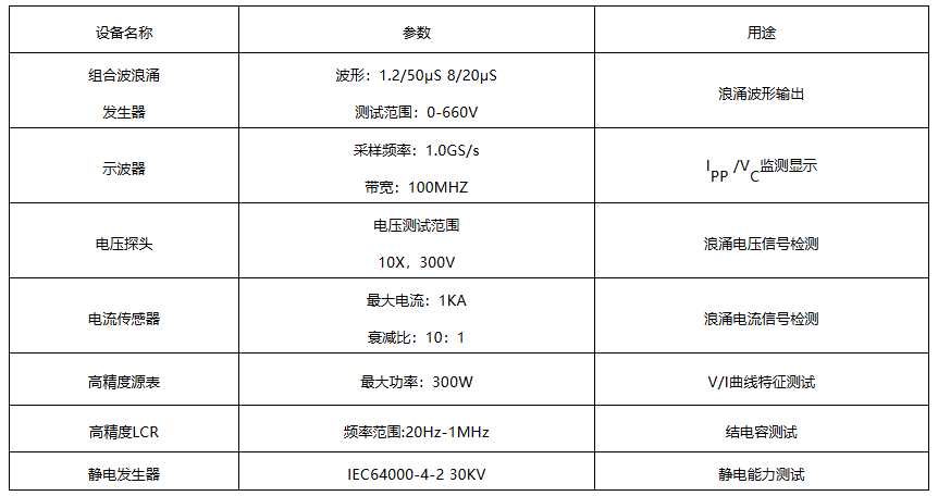
III. Static Parameter Test Comparison
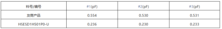
3.1 Junction Capacitance Cp
Test Conditions: VR = 100mV, f = 1MHz
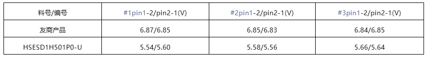
3.2 Breakdown Voltage VBR
Test Conditions: I = 1mA
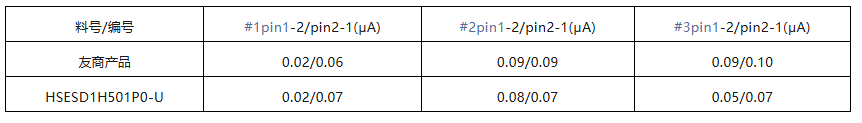
3.3 Leakage Current IR
Test Conditions: V = 3.6V
IV. Dynamic Parameters
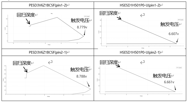
4.1.1 V/I Characteristic Curve (Voltage Source Scan)
Voltage source bias, the marked area indicates the DC voltage magnitude when the device operates, determining the device's triggering condition and scan depth under voltage bias.
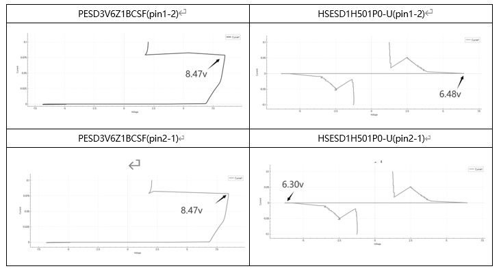
4.1.2 I/V Characteristic Curve (Current Source Scan)
Because the reverse recovery time of the PESD3V6Z1BCSF diode is relatively long, bidirectional data cannot be continuously measured for a short period of time under current bias. Therefore, its bidirectional pin is tested separately. The HSESD1H501P0-U does not have this problem.
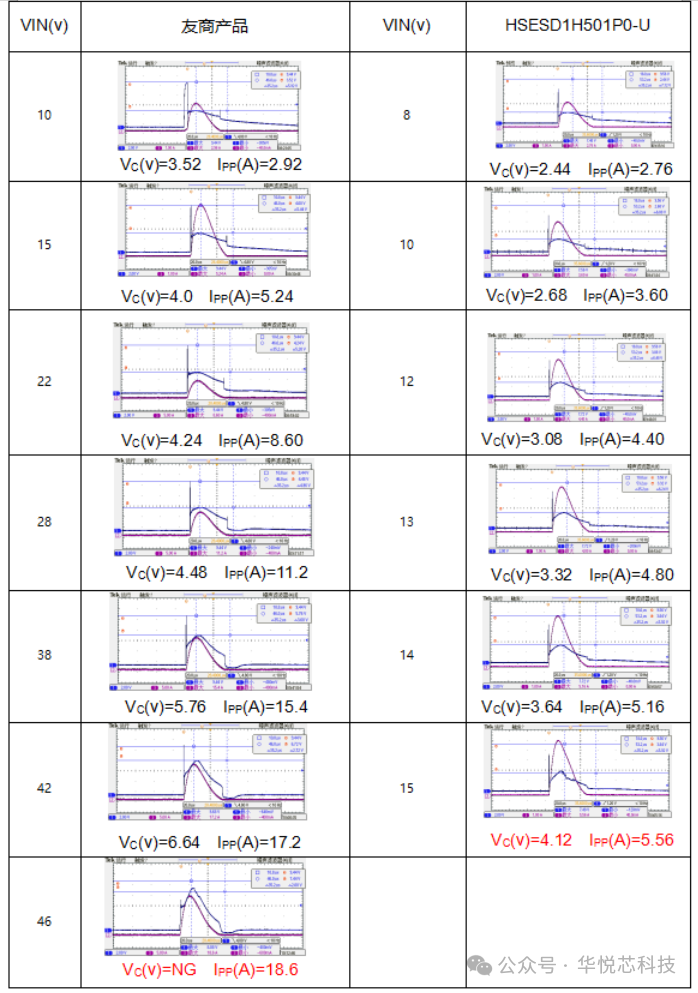
4.2 Surge Data
The test data is the average of multiple components.
Blue data represents the minimum trigger voltage and corresponding residual voltage and current for 8/20μs. Below this value, the device does not operate and is in an open-circuit state.
Red data represents the maximum trigger voltage and corresponding residual voltage and current for 8/20μs. Above this value, the device is damaged and is in a short-circuit state.
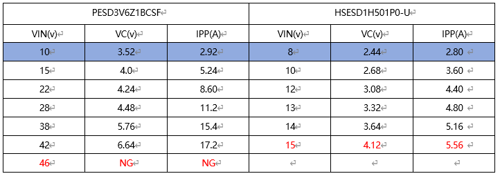
Tested under 1.2/50uS and 8/20uS combined surge generator conditions: The competitor's product did not trigger before 10V, but surge current was generated starting at 10V. The HSESD1H501P0-U triggered at 8V, generating surge current. Corresponding waveforms of the tested surges are shown below.
4.3 IEC61000-4-2 Electrostatic Discharge Capability Test. (Device powered off, one end grounded,
one end connected to an electrostatic generator)
HSESD1H501P0-U contact discharge limit: 20KV.
PESD3V6Z1BCSF contact discharge reaches the electrostatic generator limit: 30KV.
V. Comparison and Summary
Static Parameter Comparison Summary
Junction Capacitance: HSESD1H501P0-U has a lower junction capacitance than PESD3V6Z1BCSF, with typical values of 0.23pF and 0.53pF respectively. HSESD1H501P0-U offers better matching for high-speed signal transmission, better compatibility, and less impact on signal integrity.
Breakdown Voltage: HSESD1H501P0-U has a lower breakdown voltage than PESD3V6Z1BCSF and is more sensitive to current.
Room Temperature Leakage Current: No significant difference between the two.
Dynamic Parameter Comparison:
V/I Response: Using a voltage source scanning device, the HSESD1H501P0-U has a lower trigger breakover voltage and flyback depth than the PESD3V6Z1BCSF. It has a more sensitive response and better protection against voltage-type surge energy.
I/V Response: Using a current source scanning device, the PESD3V6Z1BCSF diode has a longer reverse recovery time and cannot handle reverse surge events in a short time. There is no significant difference in current discharge performance.
IEC61000-4-5 Surge Capability Test: The PESD3V6Z1BCSF has a significant advantage over the HSESD1H501P0-U, with a limiting surge current comparison of 17A:5A. Under microsecond-level surge interference, the PESD3V6Z1BCSF has stronger discharge capability.
In the IEC61000-4-2 electrostatic discharge (ESD) capability test, comparing the ESD capabilities of individual devices, the PESD3V6Z1BCSF shows a significant advantage over the HSESD1H501P0-U. The PESD3V6Z1BCSF reaches the standard equipment limit of 30KV, while the HSESD1H501P0-U's limit is 20KV.
VI. Application Recommendations
The HSESD1H501P0-U is more suitable for low-energy surge protection in high-speed communication scenarios, offering better ESD protection and less impact on signal integrity. It is more suitable for ESD protection and low-energy surge protection in high-speed communication ports.
Competitor products are limited in high-speed signal applications. They have a slower response to low-energy surges and slightly weaker protection. They are more suitable for applications with high surge current protection requirements and high ESD levels (30KV).