1. ESD TVS Technology Principles and Classification
1.1 Core Differences and Working Principles of ESD and TVS
ESD (Electrostatic Discharge Protection) transient voltage suppressor diodes are semiconductor protection devices specifically designed for electrostatic discharge (ESD) (such as human contact). Their core working mechanism is based on the avalanche breakdown effect of the PN junction. Under normal operation, the PN junction is in a high-resistance state, with only a weak leakage current (typically in the nA range) flowing through it, which does not interfere with the normal operation of the circuit.
When the circuit encounters an ESD event, the transient high-voltage pulse (with an extremely fast rise time, typically 0.7-1ns) exceeds the device's breakdown voltage (VBR). The ESD diode rapidly changes from a high-resistance state to a low-resistance state, with a response time reaching the picosecond level. During avalanche breakdown, the strong electric field causes the charge carriers within the PN junction to gain sufficient energy, impacting the crystal lattice to generate new electron-hole pairs, causing an avalanche-like increase in the number of charge carriers, prompting the diode to quickly enter a low-resistance conduction state.
The operation of a TVS diode can be divided into four stages: normal state (high resistance), transient surge state (low resistance), clamping protection, and automatic recovery. During the clamping protection stage, the diode discharges a large instantaneous current to ground while clamping the abnormal high voltage to a fixed, low level (clamping voltage VC). This voltage must be lower than the maximum peak voltage that the protected chip can withstand. Once the abnormal overvoltage disappears, the TVS diode automatically returns to the high resistance state, awaiting the next action.
The physical process of avalanche breakdown is as follows: When the PN junction is reverse biased, a small number of electrons pass through the PN junction. These electrons are accelerated by the electric field in the depletion layer, gaining significant kinetic energy. These accelerated electrons collide with atoms in the crystal lattice, ionizing them to create electron-hole pairs. The electrons in these atoms are excited to the conduction band and detach, becoming free electrons. These free electrons also accelerate and collide with other atoms, generating more electron-hole pairs, leading to further electron detachment. This phenomenon is called avalanche breakdown.
1.2 Product Classification and Structural Characteristics
ESD and TVS products can be classified into various types according to different classification standards. Based on their polarity structure, TVS diodes can be divided into unidirectional and bidirectional TVS diodes. A unidirectional TVS diode can only protect against ESD in one direction, while a bidirectional TVS diode can protect against ESD in both directions. A bidirectional TVS diode is essentially two diodes connected back-to-back; it will conduct regardless of whether the positive or negative voltage exceeds the threshold.
In terms of materials, ESD diodes are based on polymer composite materials, while TVS diodes use silicon-based semiconductor materials. Silicon-based TVS diodes are based on the PN junction avalanche breakdown principle, capable of absorbing kilowatts of surge power in ps-level time, and have no limit on the number of uses; their performance does not degrade with increasing ESD pulses.
Regarding packaging, TVS diodes offer various package configurations, including P-600, TO-218AB, SMC, SMB, SMA, SMF, and SOD-123F.
The structural characteristics of ESD diodes are also reflected in their operating voltage range and power rating. Operating voltage range from 2.5V to 36V, pulse power from 45W to 200W (8/20μs), and various package types including SOD323, SOP8, DFN1006, DFN2510, SOT23-6L, SOD523, SOT143, and SOT23-3L to meet the needs of different application scenarios.
1.3 Technical Parameter System and Performance Indicators
Key technical parameters of ESD TVS:
A. Operating Voltage (VRWM): Must be 10%-20% higher than the maximum operating voltage of the circuit (e.g., for a 5V system, select VRWM≥6V).
B. Clamping Voltage (VC): Must be lower than the withstand voltage of the protected device (e.g., if the chip withstand voltage is 10V, then VC≤8V).
C. Junction Capacitance (Cj): High-frequency signal lines require Cj < 0.5pF (e.g., USB 3.0), while power lines can be relaxed by 15pF.
D. Peak Pulse Current (IPP): Selected according to the application scenario. For example, under the IEC 61000-4-2 standard, ESD requires ≥ 30A, and lightning surge current requires even higher.
Reverse Cut-off Voltage (VRWM): This is the maximum continuous reverse voltage that the TVS can withstand in the off state. It must be higher than the normal operating voltage of the circuit. The selection principle is VRWM ≥ maximum operating voltage of the circuit × 1.2 (redundancy design).
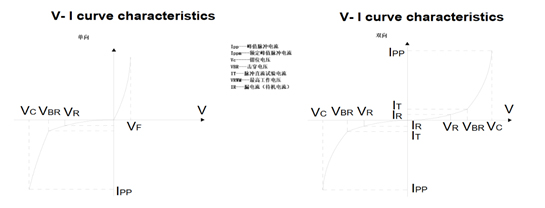
The breakdown voltage VBR is the voltage at which the TVS diode starts operating, typically the voltage at which 1mA passes through it. The applied current should generally not exceed 400ms to avoid damaging the device. The TVS breakdown voltage usually has a ±5% deviation. The clamping voltage VC is the maximum clamping voltage of the TVS when it withstands a peak pulse current (IPP). VC is typically about 1.3 times VBR.
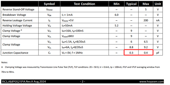
The peak pulse current IPP is a key parameter measuring the maximum transient current a TVS diode can withstand in a short time. When selecting a TVS diode, IPP ≥ 1.2 × maximum transient current should be chosen. The junction capacitance Cj mainly refers to the capacitance value of the TVS when connected to GND and I/O. For high-frequency signal lines (such as USB 3.0), Cj < 0.5pF is required, for example, RCLAMP0521PA.
In terms of response time, TVS diodes have a response time of less than 1 ns, while ESD diodes have a response time of less than 0.5 ns. Regarding power ratings, TVS diodes range from hundreds of watts to kilowatts (e.g., the SMCJ series up to 1500W), while ESD diodes have lower power ratings, commonly available in 45W, 90W, 100W, 200W, 350W, 400W, 450W, and 500W.
2. ESD TVS Selection Method and Key Parameters
2.1 Key Parameter Selection Principles
Selecting an ESD TVS requires comprehensive consideration of several key parameters. First is the selection of the reverse cutoff voltage VRWM. It must be ensured that VRWM is greater than the highest operating voltage of the protected circuit, typically 1.1-1.2 times the operating voltage, to avoid false triggering or excessive power consumption. For TVS with a VBR error of ±5%, VRWM ≈ 0.85 × VBR; for TVS with a VBR error of ±10%, VRWM ≈ 0.81 × VBR. VRWM is typically 80%-90% of VBR.
The selection of the breakdown voltage VBR is equally important; the minimum VBR must be greater than the circuit's highest operating voltage. In practical applications, the appropriate VBR value needs to be determined based on the specific operating voltage range of the circuit and potential overvoltage conditions. The clamping voltage VC is the most critical parameter in selection; VC must be less than the maximum withstand voltage of the protected device. It is generally recommended that VC ≤ 0.8 × the maximum withstand voltage of the protected IC.
The selection of the peak pulse current IPP needs to be determined based on the surge levels the circuit may encounter. For ESD diodes, attention should be paid to the 8kV contact discharge current (typically 22A, such as HSESD0541P0-N) under the IEC 61000-4-2 standard. For TVS diodes, the required IPP (inrush pressure) needs to be calculated based on the actual surge level (e.g., the 10/700μs waveform in IEC 61000-4-5). Typically, an IPP ≥ 1.2 times the actual surge current is selected.
Junction capacitance Cj is a critical parameter in high-speed signal applications. The core of ESD selection is "matching signal characteristics" to avoid conflicts between protection and signal transmission. For interfaces above 5Gbps, such as USB 3.0/HDMI 2.1, Cj < 0.5pF must be selected; for RF antenna lines, Cj < 0.3pF is required, otherwise signal attenuation and distortion will occur (e.g., RCLamp03384P).
2.2 Application-Driven Selection Strategy
Different application scenarios have different requirements for ESD TVS selection. In high-speed data interface applications, such as USB 3.0, HDMI, and DisplayPort, ultra-low capacitance ESD TVS devices need to be selected. For USB 3.0 and above interfaces, dedicated ESD/TVS devices with a Cj < 0.5pF must be selected. HDMI 2.1 interfaces require a Cj < 0.3pF (e.g., RCLamp03384P, RCLamp5031ZA).
In automotive electronics applications, CAN/LIN bus protection requires bidirectional TVS devices in SMA/SMB packages, operating at 24V-36V, with clamping voltage precisely controlled below 40V (e.g., 1.0SMBJ28CA, 1.0SMBJ30CA, SMBJ33CA are commonly used models). Automotive-grade TVS devices must meet AEC-Q101 certification and have an operating temperature range of -40℃ to +125℃. TVS diodes play a crucial protective role in automotive engine control systems, lighting systems, and battery management systems (BMS) for new energy vehicles.
In power port protection applications, systems with an input voltage range of 12V/24V must withstand surge impacts as specified in ISO 7637-2, with a peak pulse power requirement of 400W or higher. For 12V system power port load dump protection, automotive-grade TVS diodes 5.0SMDJ26CA or SM8S28CA are recommended. These are bidirectional surface mount, operating at 26V, with a clamping voltage of 42.1V, and comply with AEC-Q101 automotive-grade certification.
In industrial control applications, it is necessary to protect PLCs, frequency converters, and other equipment from back EMF surges during motor start-up and shutdown or the disconnection of inductive loads. Industrial equipment must be protected against lightning surges according to IEC 61000-4-5, with IPP reaching hundreds of amperes.
2.3 Selection Process and Decision Framework
The selection of ESD TVS should follow a systematic process. First, determine the basic parameters of the protected circuit, including maximum operating voltage, signal type (DC/AC/differential), and signal rate. Then, based on these parameters, calculate the critical parameter requirements: VRWM should be greater than the circuit's maximum operating voltage, VBR should be greater than VRWM, and VC must be less than the maximum withstand voltage of the protected chip.
When choosing between unidirectional and bidirectional structures, the signal characteristics must be considered. For DC signals (such as power lines), unidirectional devices can be used; for bidirectional signals (such as analog signals or differential interfaces), bidirectional ESD devices are required. When selecting the package type, factors such as PCB layout space, heat dissipation requirements, and automated production needs must be considered.
For high-temperature environments (such as automotive electronics), MLV (multilayer varistors) or high-temperature TVS devices with a wide operating temperature range (e.g., -40℃ to +150℃) should be selected. When selecting a specific model, the device's certification status must also be considered; for example, automotive applications require AEC-Q101 certification, while industrial applications require compliance with relevant EMC standards.
Finally, after completing the initial selection, verification and testing are required. Verification includes ensuring that VC remains below the chip's tolerance value under maximum pulse current, verifying ESD performance through testing (e.g., contact ±8kV, air ±15kV according to IEC 61000-4-2 standard), and confirming no significant degradation in signal integrity through high-speed signal testing.
3. ESD TVS Selection Guidelines for Different Application Areas
3.1 Key Selection Points for Consumer Electronics
In the consumer electronics field, ESD requirements are primarily focused on protecting various interfaces. In mobile devices such as smartphones and tablets, USB ports, headphone jacks, and charging ports are high-risk areas for ESD incidents. For these applications, low-capacitance, small-package ESD TVS devices are required.
When selecting a specific device, parameter requirements need to be determined based on the interface type and transmission rate. For example, for a USB 2.0 interface, an ESD TVS with an operating voltage of 5V and a junction capacitance requirement of less than 5pF is typically chosen. For USB 3.0 and higher high-speed interfaces, ultra-low capacitance components with Cj < 0.5pF must be selected to ensure signal integrity. ESD protection for HDMI interfaces also requires ultra-low capacitance characteristics. HDMI 2.1 interfaces require Cj < 0.3Pf (e.g., Huayuexin 4line RClamp0524PA, single HSESD0501D5-U).
ESD protection for consumer electronics must meet the IEC 61000-4-2 standard (±8kV contact discharge), with an IPP of approximately 22A (e.g., HSESD0541P0-N). In terms of packaging selection, consumer electronics products typically use ultra-small packages, such as DFN0603-2L (0.6×0.3mm), SOD-123, and SOT-23, to save PCB space.
In practical applications, Huawei, OPPO, and VIVO mobile phones use Huayuexin's SOD-123 packaged ESD diodes, providing a rapid 0.25ps response time to protect the camera and screen driver circuitry, reducing the failure rate caused by electrostatic discharge.
3.2 Selection Requirements in Automotive Electronics
The automotive electronics field has the most stringent requirements for ESD TVS diodes, demanding not only high-standard electrical performance but also rigorous reliability testing. TVS diodes play a crucial role in automotive electronic systems, including engine control systems, lighting systems, and battery management systems (BMS) in new energy vehicles.
In CAN bus protection applications, ideally, the CAN bus voltage level fluctuates between Vcc (5V or 3.3V) on the CANH line and 0V on the CANL line. As an interface, the CAN bus requires extremely reliable electrostatic discharge (ESD) protection to operate stably in the automotive environment.
Automotive CAN bus ESD protection must meet the ISO 10605 standard, which defines a waveform simulating real-world electrostatic discharge in an automotive environment. The most stringent combination is 330pF/330Ω, which is more stringent than the IEC 61000-4-2 waveform. To withstand ESD in harsh automotive environments, a minimum contact discharge rating of [insert minimum rating here] is recommended for ESD diodes. 15kV.
When selecting a transceiver, ensure the VRWM value is greater than the transceiver's recommended operating voltage range. For 12V automotive systems, a 24V ESD diode is typically chosen; for 24V systems, a 36V diode is required. All diodes must be bidirectional to handle line faults and wiring errors.
Automotive-grade TVSs must be AEC-Q101 certified, requiring 1000 temperature cycles (-55℃↔150℃), high-temperature reverse bias (HTRB 1000 hours @125℃), human body model (HBM±8kV), and machine model (MM±400V) testing. Asem's automotive-grade TVS series is AEC-Q101 Grade 0 certified and provides complete reliability test data in its datasheet, including leakage current change after ESD shock (ΔID<1μA) and clamp voltage drift (ΔVc<0.5V).
3.3 Industrial Control and Communication Equipment Selection Recommendations
TVS selection in industrial control requires consideration of harsh operating environments and complex electromagnetic interference. In industrial environments, equipment frequently faces transient overvoltages caused by motor start-stop and inductive load disconnection, as well as surge impacts from the power grid.
For industrial PLCs, frequency converters, and other equipment, protection against back EMF surges during motor start-stop or inductive load disconnection is necessary. In such applications, high-power TVS diodes are typically selected, with peak pulse power requirements exceeding 1000W (e.g., 1.0SMBJ28CA, SMDJ75CA). Industrial equipment also needs lightning surge protection according to IEC 61000-4-5 and IPP standards. Up to several hundred amperes.
In communication equipment applications, including base stations, switches, and routers, ESD is primarily used to protect various interfaces and circuits from transient overvoltages such as electrostatic discharge and induced lightning strikes. Communication equipment typically operates outdoors or in computer rooms, requiring a high level of protection.
Specific selection depends on factors such as the equipment's operating voltage, interface type, and transmission rate. For example, for Ethernet interfaces, an ESD supporting 10/100/1000Mbps transmission rates is required, with a junction capacitance below 1pF. For fiber optic interfaces, ultra-low capacitance devices are needed to avoid affecting optical signals.
Industrial-grade TVS requires an operating temperature range of -40℃ to +85℃ and must pass rigorous EMC testing, including tests according to the IEC 61000 series standards. For packaging, industrial equipment typically uses standard SOT-23 and SOD-323 packages to ensure soldering reliability and heat dissipation performance.
4. Testing Standards and Certification Systems
4.1 Overview of International Standards System
The testing standards system for ESD TVS mainly includes international and industry standards such as IEC 61000-4-2, ISO 10605, and AEC-Q101. IEC 61000-4-2 is a system-level ESD immunity testing standard applicable to electronic equipment. This standard specifies test levels of up to 8kV for contact discharge and up to 15kV for air discharge.
IEC 61000-4-2:2025 is the latest version of this standard, with several important updates compared to the 2008 version. The new standard adds calibration requirements for discharge generators, including calibration methods for air discharge modes. Regarding test setup, it explicitly requires that any external power supply to the electrostatic discharge generator be placed on a grounded reference plane (RGP), the distance between the discharge return cable and other conductive parts in the test configuration must not be less than 0.1 meters, and the impedance of the connection to the RGP and all laps should be low (e.g., ≤0.1 ohms).
ISO 10605 is a system-level standard for automotive electronic systems. The ESD testing standard, based on IEC 61000-4-2, describes vehicle-specific requirements. ISO 10605 defines various combinations of capacitance and resistance to simulate electrostatic discharge in automotive environments, with the most stringent combination being 330pF/330Ω, which is more stringent than the IEC 61000-4-2 waveform.
AEC-Q101 is an ESD testing standard developed by the Automotive Electronics Council (AEC) and is applicable to automotive devices. AEC-Q101 certification is an important certification for automotive-grade electronic components, requiring devices to pass rigorous reliability tests, including temperature cycling, high-temperature reverse bias, and ESD shock tests.
4.2 Test Methods and Acceptance Criteria
The IEC 61000-4-2 standard's test methods include contact discharge and air discharge. Contact discharge involves directly contacting the accessible parts of the device with a probe, simulating direct human contact discharge. Air discharge involves bringing the discharge electrode close to the device surface without contact, simulating discharge from a human body or object near the device.
Test levels are divided into 4 Level 4 has several levels, with contact discharge voltages reaching ±8kV and air discharge voltages reaching ±15kV, representing the mainstream compliance threshold for industries such as consumer electronics and automotive electronics. Testing requires multiple discharges at each test point on the equipment, typically at least 10 discharges per polarity.
During testing, equipment performance is evaluated in three levels: Level A (Normal Operation), meaning the product operates according to the specifications and tolerances in the product documentation; Level B (Generally Acceptable), meaning a certain degree of performance degradation is permissible during electrostatic discharge testing, provided the equipment can automatically recover to normal operation after the test; and Level C (Generally Acceptable), meaning the equipment will not be damaged during operational interruptions, and operator intervention is permitted if necessary.